13215150267
熱門關鍵詞: 光伏太陽能板天窗 防水光伏太陽能電池板 U玻璃光伏太陽能電池板









Characteristics of light
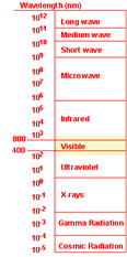
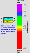
See the following figure for the wavelength distribution in each section. Visible light can be divided into purple light (390-450), blue light (450--490nm), green light (490-570nm) and red light (620-780nm)
The energy of a photon is inversely proportional to the wavelength. H is the Planck constant and C is the speed of light, both of which are constants. The following formula 1 is based on treating light as an electromagnetic wave.
Atmospheric quality: the path of sunlight through the atmosphere. AM1.5 is 1.5 times the distance of vertical incidence through the atmosphere, i.e θ= 48 degrees. Under the condition of AM0, the maximum intensity of solar energy vertically
incident on the earth is 1366w/ ㎡.
Diode and photovoltaic power generation principle
Valence band: covalent bonds bind carriers to move freely and cannot participate in conduction.
Conduction band: electrons can move freely.
Forbidden band: between valence band and conduction band.
Band gap width: the lowest energy value that an electron needs to absorb from the valence band to the free state that can participate in conduction. The band gap width of silicon material is 1.12eV, corresponding to the 110Nm band.
Carrier: both electrons and holes can participate in conducting electricity and are called.
The movement of the electron towards the conduction band results in the movement of the electron itself.
The electron movement process also produces the movement of holes in the valence band.
Intrinsic carriers: semiconductor materials without impurities that can change the carrier concentration are called intrinsic materials. The concentration is related to the material itself and temperature, and the number of electron
holes is equal.
N-type semiconductor: after doping, many subbands are negatively charged, such as phosphorus doping.
P-type semiconductor: multi subband positive charge after doping, such as boron and gallium.
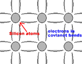
The atomic structure of crystalline silicon in which the outermost electrons are composed of four common electron pairs.
The most important parameters of solar cells
Band gap width: the minimum energy required for electron transition from valence band to conduction band;
Number of free carriers in conduction band;
The number of free carriers produced and combined under illumination.
Equilibrium carrier concentration
The intrinsic carrier concentration is determined by the material and temperature. The higher the temperature, the higher the carrier concentration.
Equilibrium carrier concentration: the number of carriers in the conduction and valence bands without bias is called the equilibrium carrier concentration. The number of multi carriers is equal to the number of intrinsic free carriers
plus the number of heterozygous free carriers. Generally, the number of heterozygous carriers is greater than several orders of magnitude of the number of intrinsic carriers, that is, it is about equal to the heterozygous concentration.
Ni: number of intrinsic carriers, n0p0 represents the number of electron and hole carriers respectively.
Light absorption:
1. Eph
2. The energy of eph=eg photon is just enough to excite an electron hole pair, and the energy is completely absorbed.
3. The photon energy of eph>eg is larger than the band gap and is strongly absorbed.
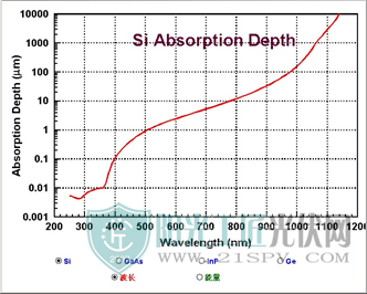
Absorption depth:
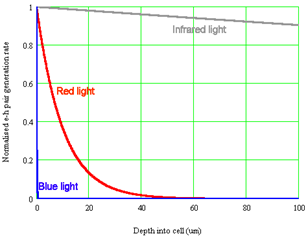
The ultraviolet band below 400nm is completely absorbed at the thickness of 0.1um.
In the visible light band of 400-800nm, it is completely absorbed at the silicon wafer thickness of 10um.
800-1000nm near-infrared band, fully absorbed at 100um silicon wafer thickness.
At 1100nm near-infrared wave band, it can penetrate the thickness of silicon wafer more than 1000um.
Carrier generation rate:
The generation rate of light at different wavelengths in the thickness of the cell: blue light is completely absorbed at 0.1um; Red light is almost completely absorbed at 50um; Near infrared light can also excite 90% of the surface
carriers at 100um, and the absorption is very slow.
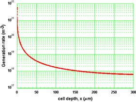
Total generation rate of full band: on the surface of the cell, the number of excited carriers is the largest because the short band is basically concentrated on the surface, and then the absorption of light decreases gradually with
the increase of the thickness of the silicon wafer, resulting in the gradual reduction of the number of carriers.
Three combinations:
? radiation recombination: the recombination of electron holes excites 1100nm light with approximate band gap width, which is also the principle of el/pl luminescence.
? Auger recombination: two electrons and one hole are involved. Electrons combine with holes to transfer energy to another electron for movement. There is no light excitation. Mainly reflected in heavily doped or heated high-temperature
materials.
? Shockley Reid hall recombination: also known as recombination of recombination centers or defect recombination, it directly absorbs electrons or holes and radiates very weak light.
Diffusion length / minority carrier lifetime
Minority carrier diffusion length: the average path of a carrier from the point of origin before recombination.
Minority carrier lifetime: the average time from generation to recombination of a carrier before recombination.
Surface compounding
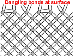
The defects on the semiconductor surface are caused by the interruption of lattice arrangement at the surface, that is, the hanging bond is generated at the surface, so the battery surface is a region with very high recombination rate.
To reduce the number of hanging keys, a thin film can be grown on the semiconductor surface to connect these hanging keys. This method is also called surface passivation.
Carrier motion: in most cases, electrons move in the opposite direction of the electric field.
Diffusion:
There will be a carrier gradient between two regions with different concentrations. The carrier will flow from the high concentration region to the low concentration region.
Drift:
The carrier motion caused by the applied electric field is called "drift motion".
PN junction:
The electron concentration in the n-type semiconductor region is very high, while the hole concentration in the p-type region is very high, so electrons diffuse from the n-type region to the p-type region. Similarly, holes diffuse from
the p-type region to the n-type region. When electrons and holes move to the other side of the PN junction, they also leave opposite charges in the impurity atom region, which are fixed in the lattice and cannot move. In the n-type region,
the positively charged nuclei are left behind. On the contrary, in the p-type region, the negatively charged nuclei are left behind. Thus, an electric field E from the positive ion region of the n-type region to the negative ion region of
the p-type region is established. This electric field region is called "depletion region", because this electric field can quickly remove the free carriers, so the free carriers in this region are exhausted.
Diode under forward bias voltage (core knowledge points)
Forward bias (also known as forward bias) refers to the application of voltage on both sides of the device to reduce the built-in electric field of the PN junction. The decrease of the electric field will destroy the balance of the
PN junction, that is, it will reduce the obstacle to the diffusion movement of carriers from one side of the PN junction to the other, and increase the diffusion current.
The increase of the diffusion motion from one end of the PN junction to the other leads to the injection of minority carriers into the edge of the dissipation region. These minority carriers gradually move away from the PN junction
due to diffusion and eventually compound with the majority carriers (multipons). The diffusion current under forward bias is also a composite current. The higher the recombination speed, the greater the diffusion current through the PN junction.
"Dark saturation current" (I0) is a very important parameter to distinguish two different diodes. I0 is a standard to measure the composite characteristics of a device. The greater the composite rate of the diode, the greater the I0.
Reverse bias
The reverse bias voltage means that an electric field is applied at both ends of the device to increase the PN junction. The larger the built-in electric field in the PN junction, the smaller the probability of carrier diffusion from
one section of the PN junction to the other, that is, the smaller the diffusion current.
Ideal diode equation:
I is the net current through the diode;
I0 is the dark saturation current (the current output without illumination), and I0 increases with the increase of T. When the temperature is 300K, kt/q=25.85mv.
V is the voltage applied to both ends of the diode;
Q and K represent the absolute value of charge and Boltzmann constant respectively;
T is the absolute temperature (k).
Collection probability: (can be compared in combination with carrier generation rate)
"Collection probability" describes the probability that the carriers generated by the light irradiating a certain area of the battery will be collected by the PN junction and participate in the current flow. Its size depends on the
distance that the photogenerated carriers need to move and the surface characteristics of the battery. The collection probability of all photogenerated carriers in the dissipative region is the same, because the electron hole pairs in this
region will be rapidly separated by the electric field. When the carrier is generated in the region where the distance from the electric field is greater than the diffusion length, its collection probability is quite low. Similarly, if the
carrier is generated in a region close to a high recombination region such as the battery surface, it will be recombined. The following figure describes the effect of surface passivation and diffusion length on the collection probability.
Quantum efficiency:
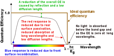
The so-called "quantum efficiency" refers to the ratio of the number of carriers collected by the solar cell to the number of incident photons. Quantum efficiency can correspond to both wavelength and photon energy. If all photons at
a particular wavelength are absorbed and the minority carriers produced by them can be collected, the quantum efficiency of all photons at that particular wavelength is the same. The quantum efficiency of photons whose energy is lower than
the band gap is zero. The following figure will describe the quantum efficiency curve of an ideal solar cell.
Photovoltaic effect (core knowledge points)
When the battery is open, the forward bias voltage of PN junction is at a new point. At this time, the magnitude of photogenerated current is equal to the magnitude of diffusion current, and the direction is opposite, that is, the total
current is zero.
When the battery is short circuited, there will be no charge accumulation, because the carriers participate in the flow of the photo generated current, and the short-circuit current is equal to the photo generated current (also equal
to the internal diffusion current under the open voltage state).
In the working state, the current is equal to the photogenerated current minus the internal diffusion current of the solar cell.
The short-circuit current is equal to the photo generated current and the drift current under the action of the built-in electric field, which is also the maximum current that the battery can provide.
Under the open circuit voltage, the photogenerated carriers cause a positive bias voltage, which weakens the built-in electric field and increases the diffusion current. The photogenerated current is equal to the diffusion current and
the direction is opposite.
In the working state, the current flowing out of the battery is equal to the difference between the photogenerated current and the diffusion current.
The built-in electric field represents an obstacle to the pre diffusion current, so the reduction of the electric field also increases the diffusion current.
Influence of composite mechanism on open circuit voltage (core difficulty)
The smaller the number of electrons at the edge of the PN junction, the wider the depletion region is, and the doping concentration needs to be increased.
Diffusion length. The higher the doping concentration, the lower the diffusion length (the greater the diffusion current), so it is necessary to reduce the doping concentration.
The two need to be balanced.
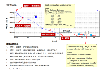
Interpretation of ECV curve
Bulk resistance (silicon wafer resistivity): the resistance is vertical, and the electrons move vertically and then reach the surface. Therefore, the moving distance is the thickness of the battery, and the cross section is the area
of the battery, i.e. R= ρ W/A
Block resistance: the resistance is horizontal, not vertical, that is, the cross-sectional area is equal to the distance L multiplied by the thickness T, so the resistance R= ρ L / (l*t). As long as l is the square side length, the
block resistance is only related to the resistivity and the thickness of N zone.
It is very easy to measure the block resistance. Through the four probe test method, the two probes outside provide current, the two probes in the middle generate voltage drop, and the PN junction between N and P regions is used as
the bonding body. Note that the test must be in a dark room.
Equivalent circuit diagram of solar cell (core knowledge points)
There are three factors causing series resistance:
First, the current flow through the emission region and the base region of the battery;
Second, contact resistance between metal electrode and silicon;
The third is the metal resistance at the top and back. The main effect of series resistance on the battery is to reduce the filling factor. In addition, when the resistance is too large, it will also reduce the short-circuit current.
The series resistance does not affect the open circuit voltage of the battery, because the total current of the battery is zero, so the series resistance is zero.
The significant power loss caused by parallel resistance RSH is usually caused by manufacturing defects.
temperature effect
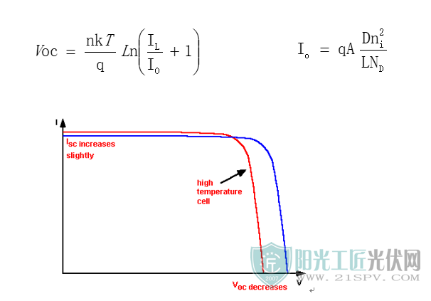
With the increase of temperature and concentration of intrinsic carriers, the dark current and recombination increase, resulting in the decrease of open circuit voltage.

 全國服務熱線
